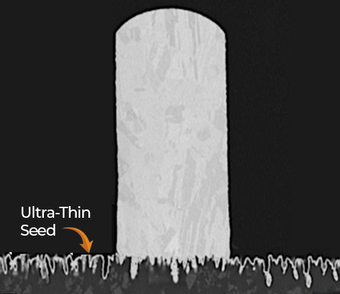
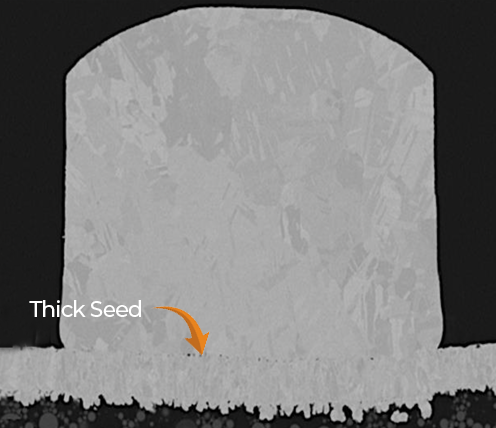
Liquid Metal Ink – LMIx® – a unique atomic seed metallization chemistry suite enabling thin, conformal deposition of palladium, copper, gold and other PCB, semiconductor and bio-compatible metals by dipping, spraying, spinning or printing.
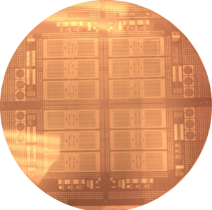
Facilitiating Direct Fan-Out
Wafer-Level Patterning
Traces printed directly on mold compound
and polyimide
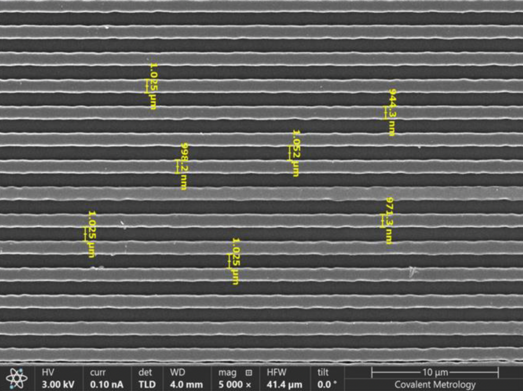
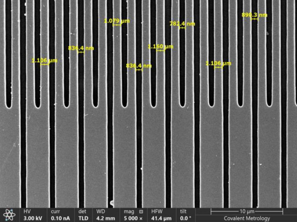
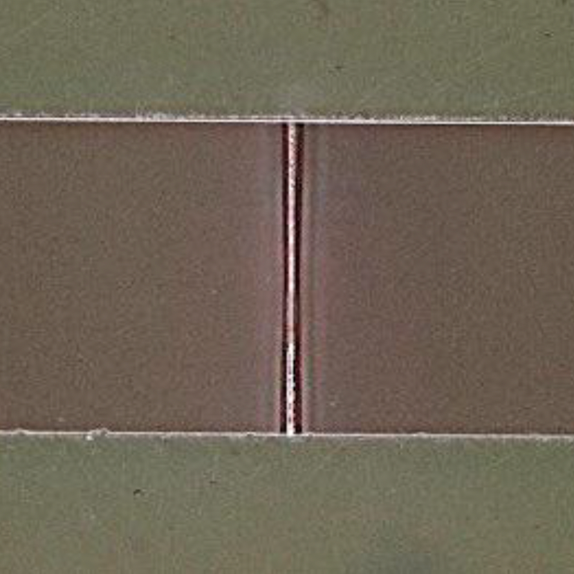
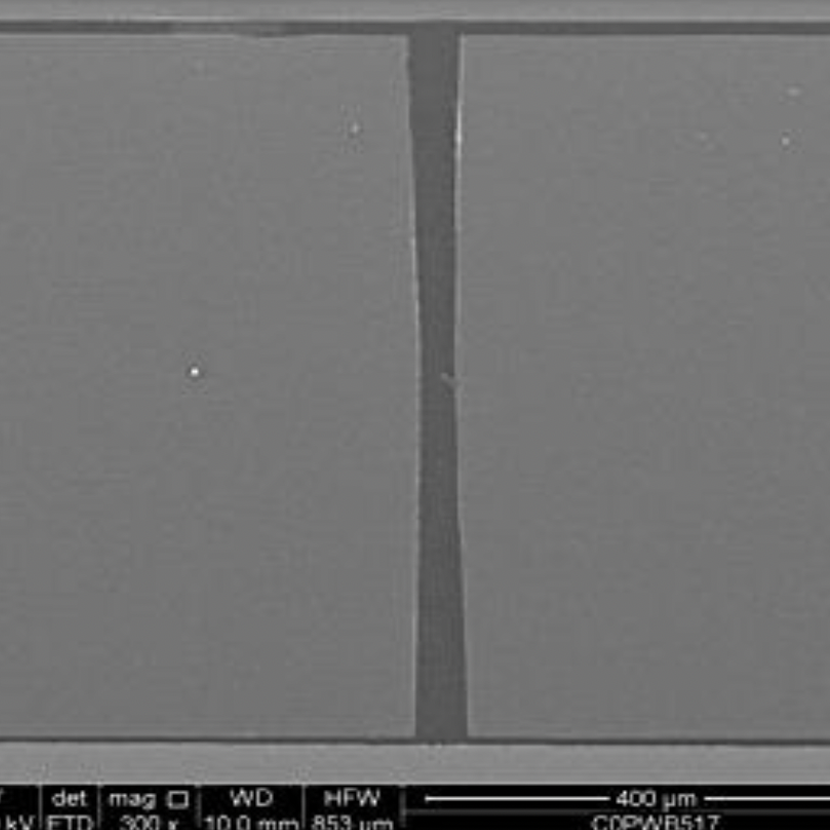
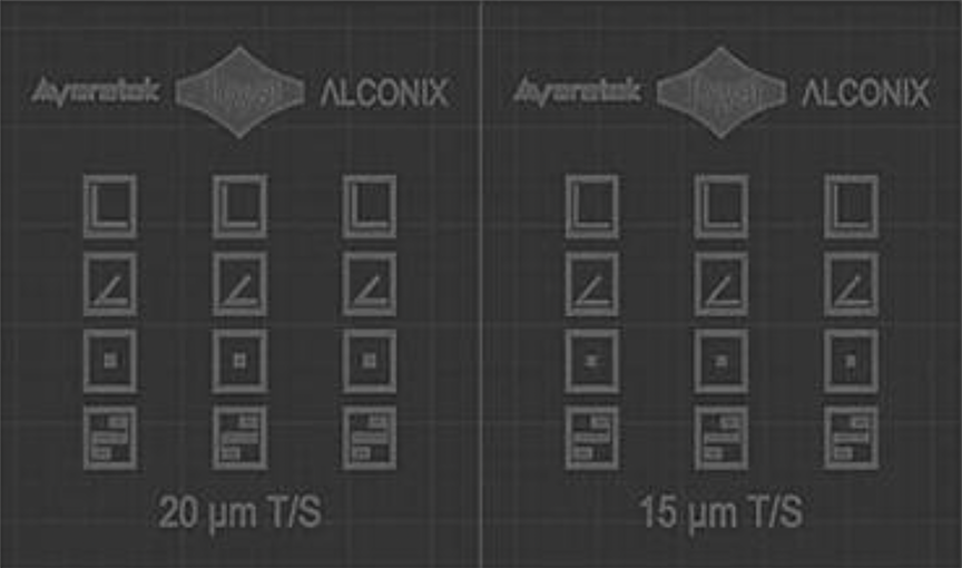
Images Shown Include:
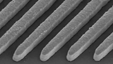
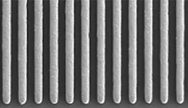
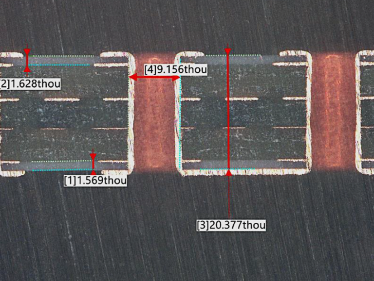
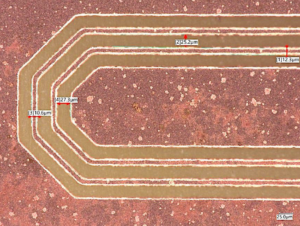
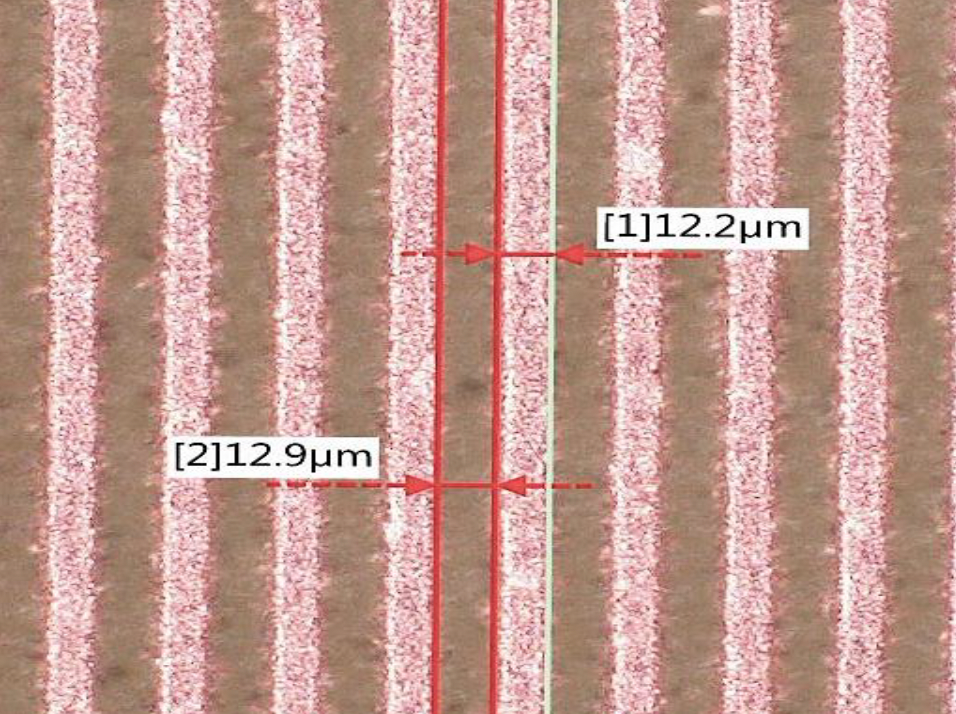
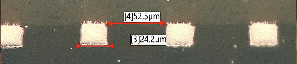
ALCONIX/LQDX: Design (7-20μm T/S)
SUMITOMO: EMC
LQDX: LMIx®
ATOTECH: E-less Cu
BREWER SCIENCE: Imaging
MARCH: Plasma
TOTECH: ECD
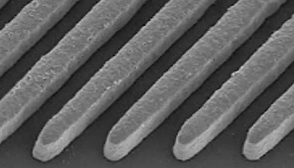
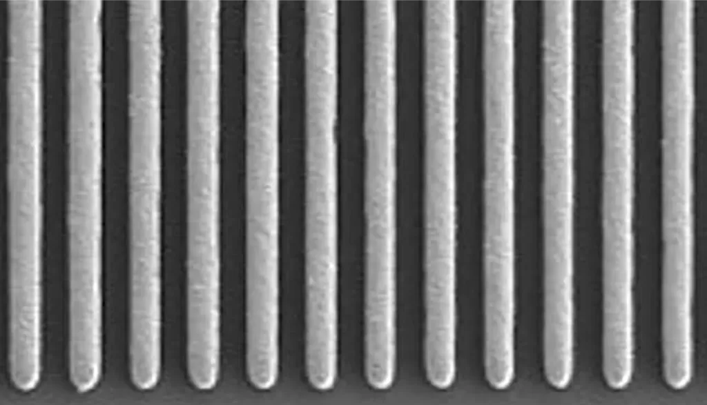
LQDX-Alconix-Brewer Science Design/Mask (7μm, 15μm, 20μm features). Max Temp 170C
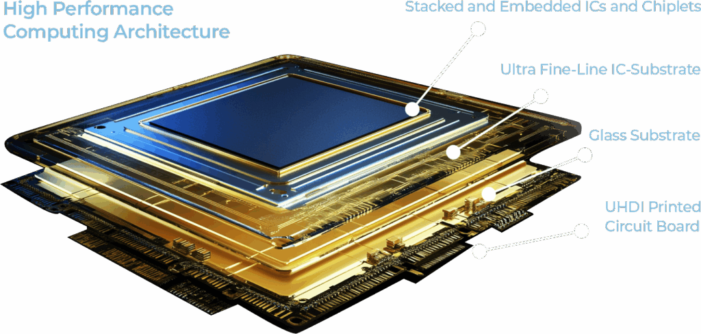
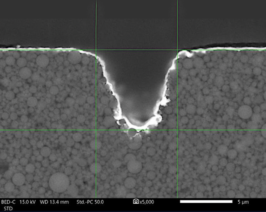
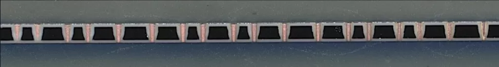
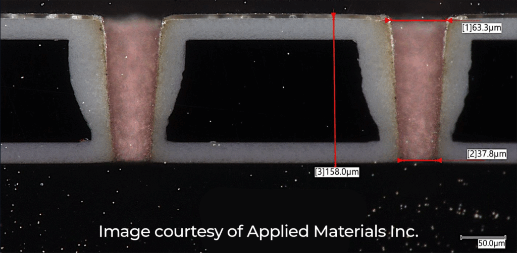
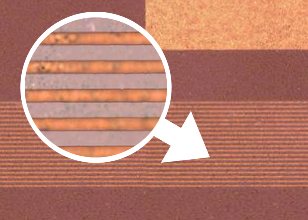
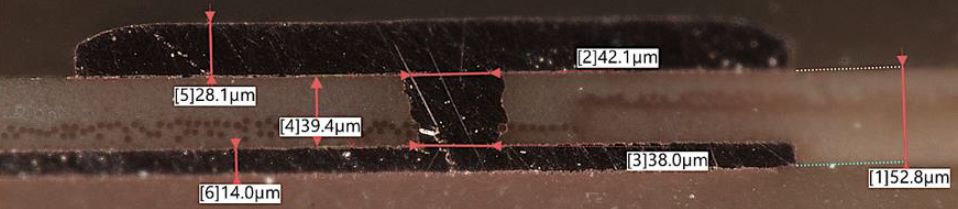
Enabling Ultra High-Density Interconnect (UHDI) PCBs Using a 100% US Supply Chain
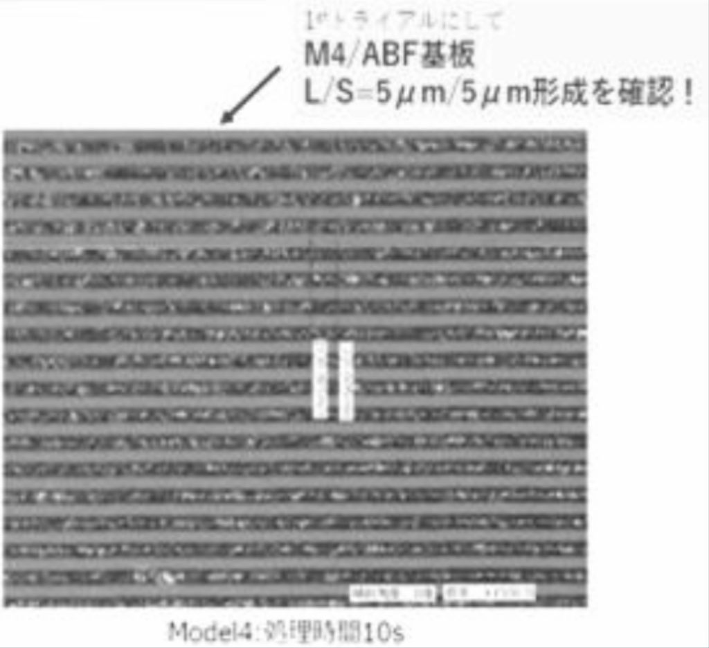
½ mil (12μm) patterns on 6-Layer UHDI RF circuit boards using 100% USA material set including LQDX ACLTM and LMI x® (Designed and built by USWC Crane)
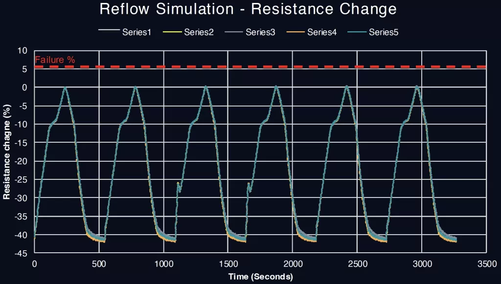
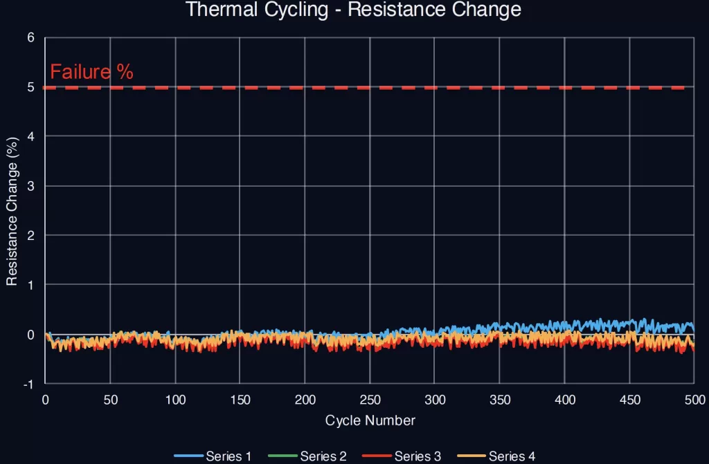
Reliability Data - Thermal Stress, Convection Reflow Simulation
Test Method: IPC-TM-650 Method 2.6.27B, Table 5-2 (230℃)
Reflow Profile: 230℃
Quantity of Cycles: 6
Number of Nets per Coupon: 2
Failure Percentage (%): 5
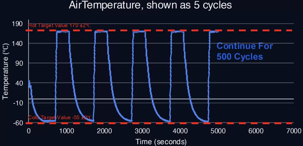
Reliability Data - Thermal Shock
Test Method: IPC-TM-650 Method 2.6.7.2C, Continuity
Cycle Range: -55℃ – 170℃
Quantity of Cycles: 500
Number of Nets per Coupon: 2
Failure Percentage (%): 5
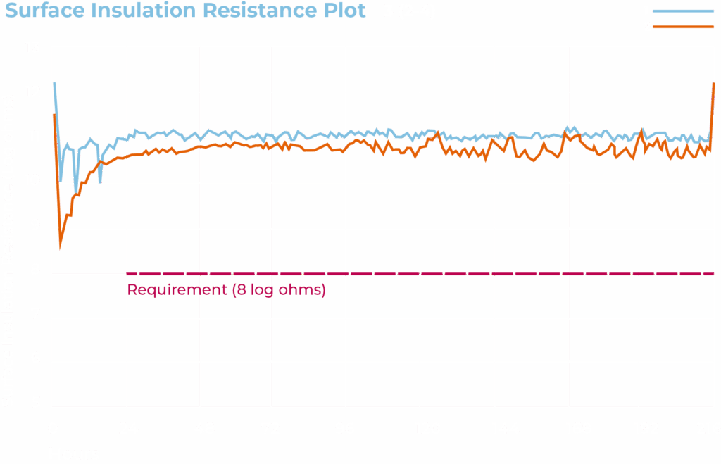
Reliability Data - Surface Insulation Resistance
Test Method: IPC-TM-650 Method 2.6.3.7
Test Conditions: 40℃ / 90%RH
Duration: 72 hours
Bias Voltage: 5 volts DC
Measurement Voltage : 5 volts DC
Requirement:
All SIR test patterns shall show a minimum resistance of 100 megohms (>108 ohms), beginning 24 hours after the chamber has stabilized at the elevated test condition.
Enabling the Next Node in
Semiconductor Interconnect
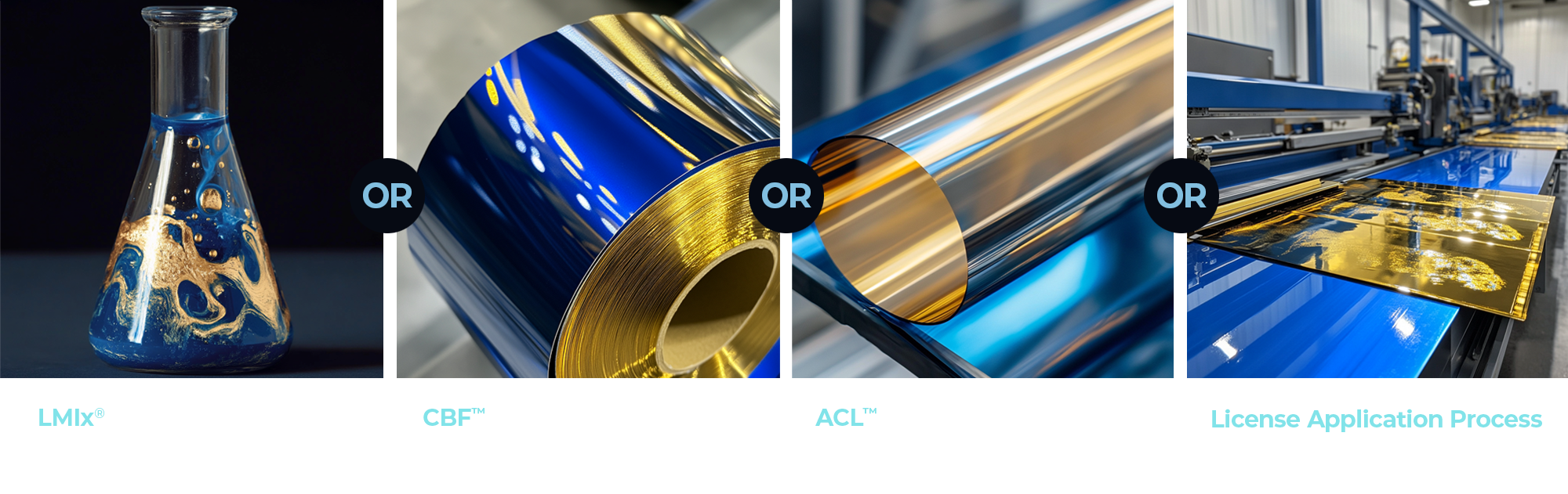
Our Technology Summarized | Products and Licensing
LQDX Technology and Product Mix
LMIx® is sold as an ink, pre-coated on laminate or flex (CBF™, ACL™), and/or as a per unit license fee for the process application (Adv-SAP™, EL-CAT™): whichever most closely fits the customer need.